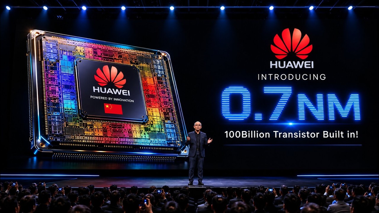
Huawei's New 0.7nm Chip Just Made Nvidia's 2nm Look Like a JOKE!
Title history
- Huawei's New 0.7nm Chip Just Made Nvidia's 2nm Look Like a JOKE! — observed on 20261031-2314 UTC (YouTube)
Keywords
Summary
178 words
Critical Evaluation
Value of the Information & Strength of the Argument
The video’s value lies in its clear explanation of a complex technical topic, demystifying the ‘0.7nm’ headline and providing a balanced perspective on Huawei’s achievements and limitations. The argumentation is solid: it builds a logical case step-by-step, from the state of the art to Huawei’s constraints and innovation, then evaluates the counterarguments. It uses specific data points (e.g., transistor density, bonding pitch, benchmark scores) and cites industry reports and analyst opinions. However, it relies heavily on Huawei’s own press releases and thin on independent verification, and sometimes uses rhetorical language that could oversimplify. The overall reasoning is coherent and informative, but the reader should be alert to the speculative elements, especially about future projections.
Scientific Rigor, Source Quality, Title Accuracy
The video demonstrates reasonable scientific rigor by referencing IBM’s official announcement, industry research firms like SemiAnalysis and Bernstein, and Huawei’s published papers. It acknowledges when information is unverified (e.g., lack of teardown) and discusses yield problems. However, it does not provide direct links to sources in the description, and some claims are drawn from unnamed supply chain reports. The title is deliberately clickbait, which detracts from the content’s credibility, though the video itself corrects the misconception. Overall, the sources are relevant and timely, but the presentation could benefit from more transparent citations and a less misleading title.
226 words
Title / Content Match
The title is sensationalist and misleading, associating a 0.7nm chip with Huawei when actually IBM made that announcement, while Huawei uses a 7nm process with folded architecture. The video dedicates substantial time to clarifying this nuance, so the content is more accurate than the title suggests.
Quality & Reliability
7/10
The video provides a detailed, well-structured analysis of Huawei's chip technology, referencing IBM, TSMC, and Nvidia, and clearly distinguishes verified facts from unverified claims. However, it relies heavily on Huawei's own statements and lacks independent verification of key metrics, leading to a moderate confidence level.
Key Moments
Markers derived by PSI from the transcript: the creator did not define chapters.
- Introduction to IBM's 0.7nm chip announcement and the distinction from Huawei's actual process node.
- Explanation that node names are marketing, not physical measurements, and overview of TSMC's 2nm production and costs.
- Huawei's history under US sanctions, the entity list, and the 2019 cut-off from TSMC and EUV tools.
- Introduction of the Tao scaling law and logic folding concept at the 2026 ISCAS conference.
- Details of the Kirin 9050 Pro chip, its specifications, and benchmark results compared to Apple and Nvidia.
- Critiques about yield, heat, and the unverified nature of Huawei's claims, including Jensen Huang's comment.
- Future roadmap for logic folding, implications for AI data centers, and the broader industry shift towards 3D stacking.
Cited Sources
- IBM announces world's first chip technology below 1nm — Mentioned as the source of the 0.7nm node claim, announced on June 25, 2026.
- Huawei's Tao scaling law paper — Published in Science China Information Sciences and pre-printed on ChinaXiv, detailing logic folding principles.
- Tech Insights teardown of Mate 60 Pro — Confirmed Kirin chip made on SMIC's 7nm process in 2023.
- SemiAnalysis teardown of Kirin 9030 — Measured metal wiring at 32.5nm and noted lower transistor density compared to Intel.
- Bernstein research on Kirin 9050 Pro performance — Provided Geekbench 6 multi-core results showing it beats A17 Pro.
Contribution & Novelties
The video contributes by connecting the dots between Huawei’s constrained manufacturing and a potential architectural breakthrough, framing logic folding as a pragmatic alternative to traditional scaling. It offers a synthesis of recent events and technical data, making complex semiconductor topics accessible. The original analysis highlights the shift from nanometer-based to efficiency-based scaling, a perspective often overlooked.
Pour aller plus loin :
- Logic folding and 3D integration — A foundational concept for stacking layers to improve performance.
- Hybrid bonding technology — The key technique enabling wafer-to-wafer connections.
- Moore’s law — The historical scaling principle that logic folding circumvents.
- Photolithography limitations — The background for why EUV machines are critical.
- Huawei’s HiSilicon division — The design arm behind Kirin chips.
118 words
Radar Profile
The radar profile shows high technical depth and information quantity but slightly lower reliability. This suggests the video is informative and well-structured but carries a moderate level of uncertainty due to unverified claims and reliance on official sources. The balance between technical detail and accessible explanation is favorable, though viewers should approach quantitative claims with caution.